

Surface Flatness and Wavefront Error
Surface Flatness Interferograms
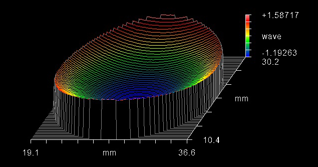
Surface flatness describes the deviation between the surface of an optical component and a perfectly flat reference plano surface. Optical filter surface flatness is measured using an interferometer (typically a laser Fizeau interferometer) that represents this deviation as a pattern of light and dark bands known as interference fringes. Interference fringes are a visual representation of the destructive interference that results from the difference in phase between light reflected off the optical filter and the reference flat. Once the interferogram is obtained, post-processing software can be used to create a 3D model of the surface.
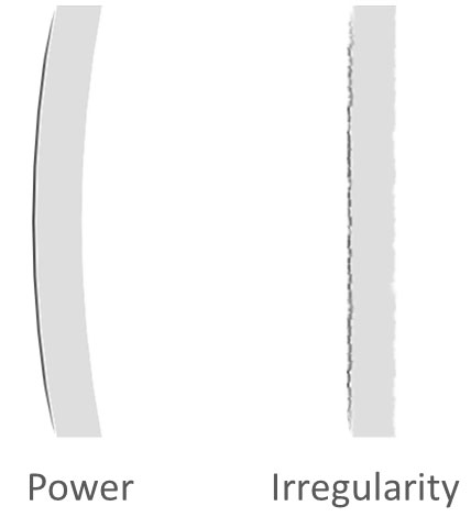
Power and Irregularity
Optical filter flatness measurements are composed of two main component properties, power and irregularity (Figure 1). Power refers to a type of spherical curvature that can result in a bowl or dome shape. On the other hand, irregularity refers to any surface deviations that are left after power, tilt, and piston are removed from the interferogram. In many cases, the remaining deviations represent small-scale surface variations, but larger deviations may still be present if irregularity wasn’t controlled during substrate fabrication. Power and irregularity can also be specified as independent surface form properties.
Although flatness measurements can either be dominated by power or irregularity, it is common for many thin-film optical filters to exhibit power-dominated flatness measurements caused by coating-stress-induced curvature. The degree of coating-stress-induced curvature will be influenced by substrate thickness, part size, and coating thickness:
$$ {δ = C \frac{L^2 h_f}{{h_s}^2} } $$Where:
- \(δ\) = Coating-stress-induced curvature, in μm
- \(C\) = Constant determined by the substrate and coating materials, dimensionless
- \(L\) = Effective Diameter (Largest linear dimension within the clear aperture), in mm
- \(h_f\) = Single-sided thin-film coating thickness or difference between surface 1 and surface 2 thin-film coating thickness, in μm
- \(h_s\) = Substrate thickness, in mm
Coating-stress-induced curvature can be minimized by multiple techniques, with the simplest being the use of a thicker substrate that will be less susceptible to coating stress. When a thinner substrate is dictated by system requirements, the next option has traditionally been to add a backside compensation coating to the filter. However, both options can introduce added cost, so Alluxa has developed a low-stress manufacturing process that is able to produce ultra-flat dichroics and mirrors without the need for backside compensation (Figures 2a and 2b).

Figures 2a & 2b: These two dichroic filters are identical in terms of spectral response, coating thickness, and both substrate thickness and material. However, the dichroic produced using the low-stress process (b) is considerably flatter than the dichroic manufactured using a standard method (a).
When to Specify Surface Flatness
Flatness specifications are typically only required when an optical component, such as a dichroic filter or mirror, is used to reflect signals to a detector. This is because coating-stress-induced curvature increases reflected wavefront error (RWE), which can result in focal shift and spot size distortion particularly in fluorescence imaging systems, laser-based fluorescence systems, total internal reflection fluorescence (TIRF) microscopes, and super resolution systems.
How to Specify Surface Flatness
Flatness can be specified in terms of either fringes or waves that correspond to the interferometer laser wavelength, which is typically 632.8 nm for many modern interferometers. When flatness is measured at normal incidence, one fringe is equal to \(λ\)/2 P-V, where \(λ\) is the interferometer laser wavelength. At non-normal incident angles, one fringe is equal to \(λ\)/2\(cosθ\) P-V.
When waves are specified, it is important to call out whether the tolerance value is peak-to-valley (P-V) or Root Mean Square (RMS). A typical flatness specification is also called out to be measured over the clear aperture (CA) of the part, but can instead be called out as “per inch” or over a smaller specified area.
It is also common to see flatness specified as Radius of Curvature (ROC), which is defined by the following formulas:
$$ { R = \frac{1}{κ} } $$
$$ { κ = \frac{8δ}{L^2}} $$Where:
- \(R\) = Radius of Curvature, in m
- \(κ\) = Curvature, in m
- \(δ\) = Coating-stress-induced curvature, in m
- \(L\) = Effective Diameter (Largest linear dimension within the clear aperture), in m
Since coating-stress-induced curvature is equivalent to measured power, \(δ\) can be expressed in terms of \(λ\) P-V by first converting to units of nm and then dividing by the interferometer laser wavelength. Therefore, in any case where optical filter flatness is dominated by power, these formulas can be used to convert ROC to \(λ\) P-V.
Reflected Wavefront Error (RWE)
Reflected Wavefront Error (RWE) is the degree of deviation seen in the wavefront when a beam is reflected off surface of an optical component compared to a perfectly flat plano surface. Surface flatness and RWE are directly related in that flatness describes the physical deviation of the optic itself, while RWE describes the resulting effect on the wavefront. When measured at normal incidence, RWE is simply equal to twice the flatness value. At non-normal incident angles, RWE = 2\(cosθ\)*flatness. Like flatness, RWE is most commonly specified in terms of waves.
Transmitted Wavefront Error (TWE)
Transmitted Wavefront Error (TWE) is the degree of deviation seen in the wavefront when a beam is transmitted through an optical component. Although wedge/parallelism, power, and irregularity all have the potential to contribute to total TWE, most definitions of TWE include only the irregularity component.
Like surface flatness and RWE, TWE is also measured using an interferometer and is most often specified in terms of waves. However, many optical filters and coatings are specified and designed with blocking in the region of the interferometer laser wavelength, making measurement impossible. In these cases, TWE can be calculated analytically using the spectral uniformity across the surface of the filter. Because spectral uniformity directly translates to coating thickness uniformity, the calculated TWE value can be added to the known TWE of the substrate, giving a relatively accurate estimation of irregularity-based TWE for the filter.
Why Alluxa?
Alluxa’s team of experts has delivered key innovations to the field of optical thin-films. In addition to designing and constructing all of our own custom optical thin-film coating equipment, we invented a novel plasma deposition coating process that both increases the performance of our optical filters and decreases the time it takes to produce them.
By combining these innovations with state-of-the-art automation, proprietary control algorithms, and precision monitoring during the coating process, we are able to deliver low-cost, high-performance, custom thin-film optical filters for any application.
